


CNC Machining for Semiconductor Equipment: Precision Parts for Wafer Processing & Chip Manufacturing
CNC Machining for Semiconductor Equipment: Precision Parts for Wafer Processing & Chip Manufacturing
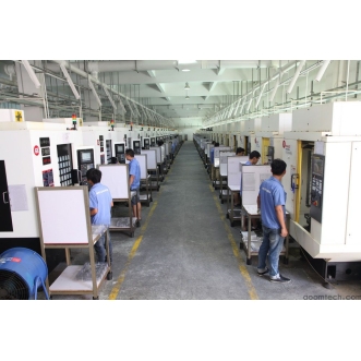
Walk into any modern fab and you'll hear it before you see it — the hum of precision machinery that turns raw silicon into the chips powering everything around us. Behind those billion-dollar lithography tools and etching chambers sits something more humble but just as critical: CNC machined components. I've spent years quoting and delivering these parts, and here's what actually matters when you're machining for the semiconductor industry.
Material Selection: What the Datasheet Won't Tell You
Every semiconductor CNC part starts with a material gamble. Aluminum 6061 carries the bulk of non-critical work — gas panels, brackets, chassis plates. It machines beautifully, chips come off clean, and you can hold tight tolerances without burning through tooling. But aluminum has a dark side in wafer processing equipment: galling. In high-vacuum environments with repeated bolt loosen-and-tighten cycles, threads can seize. I've seen a $4,000 aluminum gas distribution block scrapped because a threaded insert pulled out during reassembly.
Stainless steel 316L dominates where corrosion resistance matters — wet stations, chemical delivery modules, CMP slurry lines. The work hardening is real. You need wiper inserts and aggressive chip loads or your tool will rub and work-harden the surface mid-cut. One job I quoted for an etch chamber liner called for 316L electrolytic polished to Ra ≤ 0.2 µm. That finish pass alone ate 40% of the cycle time.
Copper and its alloys — especially OFHC (oxygen-free high-conductivity) — are the go-to for RF components machining. Waveguides, RF feedthroughs, and electrode assemblies depend on copper's conductivity and thermal performance. The problem? Copper is gummy. Stepover needs to stay under 30% of tool diameter or built-up edge forms instantly. I run PCD tooling where the budget allows.
Titanium and PEEK show up where chemical resistance meets mechanical load. PEEK is a lifesaver for wafer handling components — end-effectors, guides, suction pads. It doesn't outgas, it's cleanroom-compatible, and it handles 250°C. But PEEK machining produces long stringy chips that wrap around tool holders like fishing line. Give it a sharp tool, plenty of coolant, and never let the chip recut.
Ceramics — alumina, silicon carbide, zirconia — these are the unsung heroes of plasma-facing chamber components. They're near-impossible to machine conventionally. Diamond grinding is the only reliable route. Profiles are limited, tolerances are harder to hold, and the risk of micro-cracking during clamping is real. Worth the headache when you need dielectric properties in a 400°C plasma environment.
Tolerance and Precision: Where Microns Eat Margins
Here's the thing most buyers miss: the print tolerance isn't your real spec. A wafer processing chamber cavity called out at ±25 µm looks generous, but when you stack up thermal drift across a 12-hour machining cycle, fixture deflection from clamping force, and tool wear over 20 parts — ±25 µm gets real tight, real fast.
Cpk values tell the real story. I aim for Cpk ≥ 1.67 on any dimension flagged with a GD&T callout — usually true position or flatness on a sealing surface. For critical sealing faces on vacuum chamber parts, I've run six-hour CMM layouts across 50-point grid scans just to validate that the form didn't drift overnight.
Thermal management is the invisible battle. A 5°C shop temperature swing will shift a 300mm aluminum plate by roughly 3 µm per meter. If you're running a finishing pass at 5 PM after the HVAC cycles off for the night, your toolpath is chasing a ghost. I keep a thermocouple embedded in every critical fixture now. Sounds paranoid. Saves rework.
Surface Finish Requirements in Chip Manufacturing Components
Surface finish in chip manufacturing components isn't cosmetic — it's functional. A rough surface on a gas distribution showerhead creates micro-turbulence that kills deposition uniformity. An electrode with Ra above 0.4 µm will generate arcing in the plasma field. Catastrophic for yields.
For sealing surfaces on chamber doors and gas inlet flanges, I spec Ra ≤ 0.4 µm with no directional lay. A wiper insert on the last pass, light stepover (0.1 mm or less), and plenty of coolant. For RF components machining, surface finish directly impacts signal integrity. Mirror finishes under Ra 0.1 µm are standard. That means diamond tooling or abrasive flow finishing after the CNC cycle finishes. No shortcuts.
Cleanroom Compatibility: Beyond Just Wiping It Down
You can't just machine a part, wipe it with a rag, and call it cleanroom-ready. Every semiconductor CNC part that enters a Class 10 or Class 100 cleanroom needs a documented cleaning process. I require ultrasonic degreasing, DI water rinse, and nitrogen blow-dry — all done in a controlled environment that doesn't reintroduce particles.
The machining itself has to generate minimal burrs. Every edge break needs radii specified — sharp edges trap particles. Pockets need drain holes so cleaning fluids don't pool. Threads need to be deburred with a dedicated pass. One stray chip inside a CVD chamber and you've killed an entire batch of wafers. That scrap cost? Six figures. Easily.
Thread profiles matter in vacuum applications too. A standard 60° thread form with a sharp root is a leak path waiting to happen. Unified or buttress threads with radiused roots seal far better. I've rejected three consecutive batches of O-ring gland depths because they were 0.05 mm off — that's the difference between a seal and a vacuum leak.
Quality Systems and Certifications That Actually Matter
ISO 9001:2015 — baseline, table stakes. If your supplier doesn't have it, run. But for semiconductor work, ISO 13485 (medical device standard) is increasingly the real benchmark. The traceability requirements, document control, and risk management processes map directly to what a fab expects from its parts suppliers.
Every batch I ship includes material certs with traceable heat numbers, dimensional inspection reports with actual measured values (not just pass/fail), and surface finish data from a profilometer — not a visual comparison. If the drawing calls out a surface texture requirement, I deliver the Ra, Rz, and Rmr data.
ESD-safe packaging, moisture barrier bags, and cleanroom double-bagging with lot-specific labels. That's not paperwork — that's how parts survive the logistics chain from the machine shop to the fab floor without accumulating contamination they'll never lose.
Design for Manufacturing: The Conversations That Save Everyone Money
The most expensive micron you'll ever cut is the one the design engineer didn't need. I've opened countless solid models where a sealing surface carried a ±5 µm tolerance on a feature that sits against a compression gasket. Gaskets compress 30%. That tolerance buys nothing.
Design engineers who understand GD&T are the ones who get scrapped parts within spec. A true position callout with MMC (maximum material condition) on bolt holes saves my tooling and your lead time. A generous corner radius instead of a sharp internal corner lets me use a standard end mill instead of a special grind. Simple stuff that saves thousands.
When I evaluate a semiconductor CNC part print, here's my mental checklist: Is the material available with traceable certs? Can the surface finish be achieved without a secondary operation? Is the feature accessible with a 4th axis or does it require a 5th? Are there thin walls that'll chatter during the finishing pass? One part I quoted had 1.2 mm walls on a 316L gas manifold — required three roughing passes and a dedicated finishing pass with reduced radial engagement just to avoid pushing the wall into the next time zone.
Fixture deflection is the silent killer of precision. A 0.05 mm deflection at the jaw translates to a tapered cut across a 200 mm face. Soft jaws, carefully torqued, with locators that reference previously machined surfaces. I tell every engineer who asks: if you want ±10 µm on a part, design a datum scheme that my CMM can find without guesswork.
Vacuum Chamber Parts: Sealing, Leak Rates, and the Hidden Costs
Vacuum chamber parts live in a different world. A static seal for a gate valve has to hold 1×10⁻⁹ Torr. That's not a machining tolerance you can see with your eyes — it's a surface finish so smooth that the Ra value is measured in nanometers. The seal groove geometry has to be dead-nuts on depth and width. Too deep and the O-ring over-compresses, too shallow and it extrudes.
Helium leak testing after machining is non-negotiable. I've run parts that passed a 1×10⁻⁹ std cc/s leak check and still failed on the second test — because of thermal cycling relaxing residual stresses that were locked in during roughing. Stress relief before finishing is expensive. A rejected chamber after assembly is catastrophic.
RF components machining adds another layer. Electrical conductivity, skin depth, surface roughness all affect RF power delivery. A copper electrode with a milled surface at Ra 0.8 µm will have 15% more RF loss than one polished to Ra 0.1 µm. That loss dissipates as heat. Heat shifts your plasma chemistry. Hard to hold critical dimensions when your chamber temperature is drifting.
The breakthrough for semiconductor precision machining has been temperature-controlled coolant systems — within ±0.5°C — running through the spindle and the fixture. Combined with CMM feedback loops that adjust tool wear offsets mid-program, you can hold Cpk of 2.0 across large production runs. That's the kind of process control that chip manufacturing components demand.
At the end of the day, machining for the semiconductor industry is about trust. Every part leaves the spindle holding a piece of the fab's yield in its dimensions. Get the surface finish wrong on a wafer guide — you scratch a $300 wafer. Get a chamber wall flatness out of spec — you lose vacuum and kill a thousand-wafer batch. The margins are tight, the tolerances are unforgiving, and the materials fight you every step of the way. That's exactly why I love this work.
— Published by AOOM Technology. Need precision semiconductor CNC parts for your next project? Let's talk.
 CNC Machining for Semiconducto
 5-Axis CNC Machining: A Comple
 High Volume CNC Machining: Str
 CNC Machining for Robotics: Pr