


CNC Machining Process for Precision Parts of Semiconductor Equipment
The CNC machining process for precision parts of semiconductor equipment is very different from general industrial machining. In this field, a part is not judged only by size. It must also control particles, surface condition, corrosion, flatness, and repeatability. Semiconductor manufacturing is highly sensitive to contamination, and industry sources note that particles, metal ions, chemicals, bacteria, and airborne molecular contaminants can all hurt yield and reliability. Cleanroom standards such as ISO 14644 also treat cleanrooms as spaces designed and operated to control particle introduction, generation, and retention.
That is why buyers and engineers often face the same problems: a part meets drawing dimensions but fails cleanliness, a low-cost material corrodes in plasma, or a wrong tool leaves burrs and smearing that later become contamination sources. A better process starts early, with clear function-based specifications for the part, then matches the material, tooling, finishing, cleaning, and inspection method to the real job the part will do inside the equipment.
Why Semiconductor Equipment Parts Need a Special CNC Process
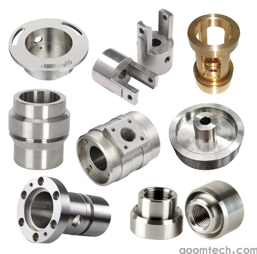
Semiconductor equipment uses many different precision parts, including showerheads, pedestals, weldments, optical housings, electrostatic chuck parts, quartz chambers, wafer boats, wafer handling arms, gas feed flanges, and vacuum chuck components. These parts work in difficult environments such as vacuum, plasma, chemical wet processing, high-purity gas delivery, and fine wafer handling. Because of that, the machining process has to protect both dimensional accuracy and process cleanliness.
For example, Kyocera explains that semiconductor processing equipment needs ceramics with high rigidity in lithography equipment, plasma resistance and low particle generation in etch and deposition equipment, and high precision in wafer transfer arms. ACCRETECH also notes that on electrostatic chucks, surface roughness affects adsorption force and thermal control, while flatness and parallelism help hold wafers level. This shows an important point: in semiconductor tools, geometry and surface quality directly affect process performance, not just assembly fit.
In practice, this means a good machining plan should separate features into three groups: critical functional features such as sealing faces, wafer contact areas, and optical or motion interfaces; critical cleanliness features such as fluid paths and chamber-facing surfaces; and general structural features such as non-critical mounting surfaces. This simple step helps reduce cost, because not every face needs the same tolerance, finish, or cleanliness level. That is a practical way to avoid over-engineering while still protecting yield-sensitive functions. This is an engineering inference based on how standards and equipment suppliers define critical chamber components, wetted surfaces, and functional measurement targets.
Precision Requirements in CNC Machining Semiconductor Equipment Parts
When people discuss precision requirements in CNC machining semiconductor equipment parts, they often think only about a tight dimensional tolerance. In reality, the job is wider. Many semiconductor parts must control size, position, flatness, parallelism, roundness, burr level, surface roughness, and cleanliness all at the same time. ISO 14644 also notes that controlled environments may need attention not only to particles, but also to temperature, humidity, pressure, vibration, and electrostatic effects.
Surface texture can be especially important. Swagelok’s ultrahigh-purity process specification points to SEMI F19 and SEMI F37 for surface condition and roughness measurement of wetted stainless-steel surfaces, and SEMI F57 for polymer components used in ultrapure water and liquid chemical systems. The same document states that many of its ultrahigh-purity stainless wetted surfaces are produced at Ra 5 μin. or 0.13 μm, while its ultrahigh-purity plastic products are machined to a maximum Ra 25 μin. or 0.62 μm. These are product-specific values, not universal rules, but they show how smooth the surface may need to be once a part enters a high-purity fluid path.
For semiconductor-facing hardware, poor surface control can create real process problems. ACCRETECH states that roughness on electrostatic chuck surfaces affects adsorption force and thermal control, and that quartz boats and related quartz parts can cause process abnormalities if the wafer guide pitch, contact areas, and fixing features are not properly controlled. In other words, the drawing should clearly say which surfaces matter most, because the machinist cannot guess that from a basic 3D model alone.
A useful rule for buyers is simple: if a feature touches the wafer, faces plasma, seals vacuum, carries high-purity gas or chemicals, or sets optical or motion accuracy, mark it as critical on the drawing and define the inspection method in advance. If a feature only holds the assembly together, use a normal industrial tolerance unless there is a proven reason to tighten it. This reduces scrap, rework, and unnecessary machining time. That recommendation is a practical manufacturing inference built on the equipment functions and standards above.
Material Selection for CNC - Machined Semiconductor Precision Parts
Material selection for CNC - machined semiconductor precision parts should always start from the service environment, not from stock price alone. The same chamber may have structural parts, fluid-path parts, wafer-handling parts, and plasma-facing parts, and each group may need a different material. A wrong material can create corrosion, particle shedding, ionic contamination, or unstable geometry.
Aluminum alloys are common when light weight and machinability matter. A 2020 coatings study states that aluminum is often used in semiconductor equipment parts because it has high ductility and excellent machinability, but it also notes that aluminum can corrode in fluorine plasma and create contaminant particles. Published semiconductor processing patents and studies therefore describe anodic aluminum-oxide films as a common protection method for plasma-exposed aluminum parts. For aluminum chamber or plate parts, a good process often includes rough machining, stress control or stabilization if needed, final machining, then anodizing or another approved coating.
Stainless steel and corrosion-resistant alloys are widely used for ultrahigh-purity gas and chemical delivery, fittings, valve bodies, and vacuum hardware. Swagelok states that electropolishing smooths the surface and removes metallic impurities, while passivation creates a chromium-rich passive oxide layer that improves corrosion resistance. Its semiconductor products also include 316L VIM-VAR stainless steel and Alloy 22 options for aggressive media. If a part will carry high-purity process gas or chemistry, stainless is often chosen not because it is easy to machine, but because it supports cleanliness, corrosion resistance, and stable surface finishing.
Engineering plastics are a strong choice when low weight, chemical resistance, insulation, or low metal contamination is needed. Ensinger shows semiconductor examples of PEEK, PPS, PVDF, and ESD-safe materials for wafer holders, clamp rings, vacuum wands, gas feed flanges, and wet-process parts. Drake Plastics adds that PEEK has good chemical inertness, inherent purity that helps minimize ionic contamination, and very low erosion in plasma gases. Victrex also describes PEEK as a high-performance polymer with strong chemical resistance over a wide temperature range. These points make PEEK and similar materials useful for wafer handling, wet process fixtures, and selected plasma-adjacent parts.
Ceramics, quartz, and sapphire are often better for the hardest environments. Kyocera states that semiconductor equipment uses ceramics where plasma resistance, low particles, heat resistance, low dielectric loss, high precision, and high rigidity are needed, and lists examples such as electrostatic chucks, domes, chambers, polishing plates, vacuum chucks, lift pins, and sapphire chamber windows. For these materials, fully conventional metal-style CNC machining is often not the only answer. CeramTec notes that machining after sintering is much more difficult, and final grinding, lapping, polishing, and drilling are used when very tight tolerances and smooth surfaces are required.
A practical material map looks like this:
Aluminum: good for structural plates, housings, chamber bodies, and other parts that need low weight and fast machining, but plasma-facing use usually needs a qualified protective coating.
316L stainless or higher alloys: good for ultrahigh-purity gas, chemical, and vacuum hardware where corrosion resistance and electropolished surfaces matter.
PEEK, PPS, PVDF, PTFE-based plastics: good for wet process, wafer handling, ESD control, and selected low-contamination fixtures.
Ceramics, quartz, sapphire: good for plasma resistance, high rigidity, thermal stability, and low-particle semiconductor process zones.
Tooling Options for CNC Machining Semiconductor Equipment Components
Tooling options for CNC machining semiconductor equipment components should be chosen by material and by contamination risk. A tool strategy that works for general machinery can be a bad choice for semiconductor parts if it creates burrs, smearing, extra heat, or unstable tool wear. The goal is not only cutting speed. The goal is predictable edges, stable surfaces, and repeatable cleanliness.
For aluminum, Sandvik Coromant advises sharp, polished PCD-tipped or positive-geometry tooling to resist built-up edge and improve chip formation. It also recommends cutting fluid for aluminum milling to reduce smearing and improve surface finish. This matters for semiconductor housings, plates, gas distribution parts, and shower-type hardware, where a smeared edge or burr can later become a particle source.
For stainless steel, the problems are different. Sandvik notes that austenitic and duplex stainless steels can suffer from thermal cracking, edge chipping, built-up edge, burrs, and poor surface finish. Its guidance for roughing uses higher cutting speeds to avoid built-up edge, while finishing may still use coolant or minimal lubrication to improve the finish. It also highlights dedicated stainless grades that resist heat-related wear. In simple terms, stainless needs a tool and parameter set that controls heat and work hardening, not just brute cutting force.
For drilling and intersecting holes, polished-flute carbide drills can help chip evacuation, hole quality, and heat control. Sandvik states that polished flutes improve chip evacuation, reduce cutting forces, reduce heat build-up in the tool, and improve finished hole quality. That is useful for manifold blocks, distribution plates, and precision mounting plates, which are common part families in semiconductor tooling.
For PEEK and other high-performance plastics, heat and fixturing become the main issues. Drake Plastics states that PEEK is stiffer than many plastics but softer than metals, so fixturing is critical. Its machining guide recommends carbide tooling for short runs, PCD tooling for long runs or reinforced grades, low-helix drills plus flood coolant for deeper holes, and climb milling with positive-geometry cutters to lower heat build-up and improve chip removal. This is a good example of why a shop that mainly cuts metal may still struggle with semiconductor plastics if it does not adjust tooling and workholding.
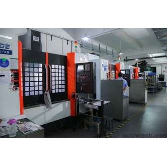
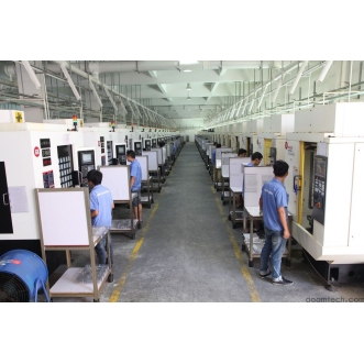
Machine choice also affects result quality. Where a part has many sides, deep pockets, seal grooves, and angle features, 5-axis machining can reduce set-ups and support better access. Makino states that 5-axis machining offers fewer set-ups, full-part access to complex geometries, and better surface finish that can reduce downstream processing. For simpler aluminum semiconductor equipment parts, Brother also highlights machining-center productivity and process integration. In practical terms, if a housing or plate can be completed in one or two secure fixtures instead of four or five, the risk of stack-up error and handling damage goes down.
Contamination Prevention in CNC Machining Semiconductor Parts
Contamination prevention in CNC machining semiconductor parts is not a final cleaning step alone. It starts with the whole process chain. Swagelok’s cleanliness guidance warns that machining oils and coolants, finishing media, and electropolishing electrolytes can all compromise purity if they are not fully removed. SEMI also notes that particle contamination on critical chamber components can badly affect wafer yield and device reliability.
A practical contamination-control plan usually includes dedicated material storage, clean fixturing, controlled deburring, controlled coolant use, and a cleaning route matched to the part material and service. For example, semiconductors are sensitive to particles and chemical contamination, while KRISS reports that corrosion of internal process-chamber parts can create fine contaminant particles that fall on wafers and reduce performance. This is why “dimensionally correct” is not enough in semiconductor machining. If corrosion, burrs, or residues remain, the part can still fail in real use.
Final cleanliness should also be measured in a repeatable way. SEMI describes two notable approaches for critical chamber components: ultrasonic-aided deionized or ultrapure water extraction followed by liquid particle counting, and adhesive replacement-substrate testing followed by optical metrology and SEM/EDX analysis. The extraction method described by SEMI is carried out in a certified ISO 6 cleanroom environment. These methods matter because they turn a vague request like “make it clean” into a measurable requirement.
Packaging is part of contamination control too. Swagelok states that packaging should prevent outside contamination during shipping and should keep identification visible without opening the package. Its ultrahigh-purity tubing documentation also describes capped, purged, and double-bagged products handled in an ISO Class 4 cleanroom. Not every machined part needs that exact packaging level, but the lesson is clear: if you open the bag to identify the part, you already created an avoidable contamination risk.
For buyers, the easiest way to reduce problems is to place cleanliness on the drawing and PO in plain language. Ask for the cleaning method, the allowed residue or particle test method, the packaging method, and the traceability label format. If those points are missing, the supplier may deliver a good-looking part that is not ready for a semiconductor tool. This recommendation is a practical inference from SEMI and Swagelok documentation on standardized measurement, packaging, and communication between suppliers and users.
Inspection and Quality Control for Release
The best CNC process still needs a strong release plan. At minimum, semiconductor equipment parts usually need material traceability, dimensional inspection, geometric inspection where needed, surface-finish checks, and cleanliness confirmation matched to the application. Swagelok’s ultrahigh-purity process specification, for example, ties roughness verification to ASME B46.1 and includes verification methods for surface condition and appearance.
For size and form, coordinate measuring machines remain a common choice. ACCRETECH states that it uses high-precision scanning-probe CMM solutions for dimensional measurement and geometric tolerance evaluation of quartz glass parts used in exposure, cleaning, diffusion, deposition, ionization, and etching equipment. It also emphasizes the need to control flatness and parallelism on electrostatic chuck-related parts and surface roughness on wafer-holding surfaces.
For vacuum and high-purity gas hardware, leak integrity can also be part of final release. Swagelok’s semiconductor materials pages and VCR fitting data describe helium leak performance suitable for vacuum and high-purity gas systems, and its ultrahigh-purity products are built around controlled surface finish and clean operation. For a machined manifold, fitting body, or welded assembly, it is wise to define early whether helium leak testing is required, because that changes both process flow and cost.
A useful release package for a precision semiconductor part often includes the following:
Material certificate and heat or lot traceability for the raw stock or molded shape.
Dimensional and geometric report for critical features, not just a general statement of compliance.
Surface-finish report for sealing, wetted, wafer-contact, or optical surfaces when specified.
Cleanliness or particle test report when the part is chamber-facing, fluid-path, or otherwise critical to yield.
Packaging and label record so the part can move into cleaning, assembly, or fab support areas without unnecessary repacking.
Practical Steps to Make the Process More Reliable and Cost - Effective
If you want a CNC machining process for precision parts of semiconductor equipment that is both reliable and cost-aware, the main idea is simple: put the highest controls only where the process truly needs them. Semiconductor parts do need strict standards, but not every hole, face, and corner should be treated like a wafer-contact or gas-wetted surface. Classify features by function, choose materials by environment, choose tools by material behavior, and define cleanliness in a measurable way.
For many teams, these actions bring the fastest improvement:
Mark critical surfaces on the drawing. Identify wafer-contact, plasma-facing, sealing, vacuum, optical, and ultrahigh-purity fluid-path features separately from general structure.
Choose the material after reviewing the real service environment. Plasma, wet chemistry, high-purity gas, ESD, and thermal stability often matter more than simple machinability.
Use the right tooling for each material family. Aluminum often benefits from sharp polished tooling, stainless needs heat and work-hardening control, and PEEK needs careful fixturing and heat management.
Reduce set-ups where possible. Multi-axis machining can lower stack-up error and help surface consistency on complex parts.
Specify cleanliness and packaging in writing. If the only requirement is “clean before ship,” different suppliers may interpret it very differently.
Match inspection to risk. Use full documentation for critical features and avoid paying for excessive inspection on non-critical geometry. This is a practical cost-control inference from the standards and application-specific measurement practices above.
In short, the most successful suppliers are not the ones that only promise “tight tolerance.” They are the ones that understand precision requirements in CNC machining semiconductor equipment parts, can justify material selection for CNC - machined semiconductor precision parts, know the correct tooling options for CNC machining semiconductor equipment components, and build real contamination prevention in CNC machining semiconductor parts into the full workflow from raw stock to final bagging.
 How to Ensure Precision in CNC
 Small Batch Precision CNC Mach
 What surface finish can CNC ma
 CNC Machining Tolerance Settin