
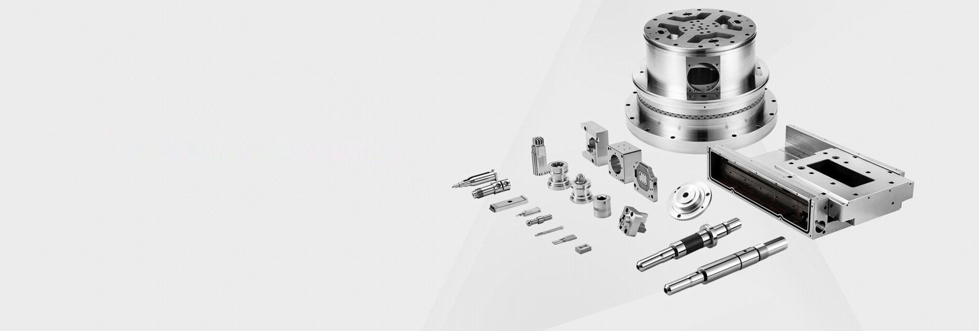
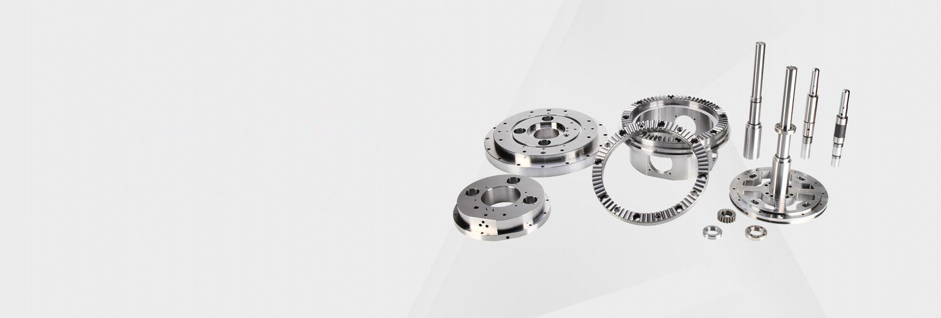
CNC Machining Process for Precision Parts of Semiconductor Equipment
The CNC Machining Process for Precision Parts of Semiconductor Equipment is one of the most demanding manufacturing processes in modern industry. Semiconductor devices, such as microchips and wafers, require extremely clean, stable, and highly accurate equipment to produce circuits at nanometer and sub-nanometer scales. Even the smallest machining error in equipment parts can affect wafer alignment, contamination control, and production yield.
In this field, machining precision often reaches sub-micron tolerances (less than 1 micron). This level of accuracy is critical because semiconductor manufacturing processes like lithography, etching, and deposition depend on perfect mechanical stability and alignment. Any vibration, surface defect, or dimensional deviation can lead to defective chips and significant production losses.
Materials for Semiconductor Equipment Parts
Choosing the right material is a key step in semiconductor manufacturing. The materials for semiconductor equipment part CNC machining must offer excellent thermal stability, chemical resistance, and ultra-clean performance.
High-Purity Ceramics
High-purity ceramics such as alumina (Al₂O₃) and silicon carbide (SiC) are widely used. These materials provide excellent electrical insulation, high wear resistance, and strong chemical stability. They are ideal for wafer handling parts and insulating components inside vacuum chambers.
However, ceramics are brittle and can easily crack during machining. This requires very careful control of cutting forces and tool selection.
Silicon-Based Materials
Silicon carbide and other silicon-based advanced materials are used in high-temperature and high-precision environments. They offer strong thermal conductivity and stability, making them suitable for components exposed to plasma or high-energy processes.
Specialized Metals
Stainless steel (high-grade vacuum-compatible types), aluminum alloys, and nickel-based alloys are also common. These metals are used for structural frames, vacuum chambers, and motion systems. They provide strength, corrosion resistance, and good machinability when properly controlled.
Pre-Machining Preparation
Accurate Design and CAD/CAM Programming
A successful CNC Machining Process for Precision Parts of Semiconductor Equipment begins with extremely accurate design work. Engineers create detailed 3D CAD models that define every dimension, tolerance, and surface requirement.
In semiconductor applications, tolerances are often in the sub-micron range, so even tool path planning must consider tool deflection, thermal expansion, and vibration effects.
Advanced CAD/CAM simulation is essential. It helps detect issues such as:
Tool-part collisions
Excessive tool deflection
Improper cutting angles
Thermal deformation risks
Machine Setup and Calibration
Machine setup is another critical step. CNC machines must be carefully calibrated before production begins. Key actions include:
Aligning machine axes with high precision instruments
Checking spindle run-out (must be extremely low, often below a few microns)
Verifying tool changer accuracy and repeatability
Ensuring thermal stability of the machine environment
A clean machining environment is essential. Even microscopic dust particles can affect semiconductor parts, so machining is often performed in controlled cleanroom conditions.
CNC Machining Operations
Ultra-Precision Milling
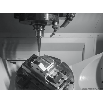
Ultra-precision milling in semiconductor part machining is used to produce complex geometries such as alignment platforms, wafer chucks, and micro-structured surfaces.
This process uses high-speed spindles and extremely sharp cutting tools. The goal is to minimize cutting force while achieving mirror-like surface finishes.
Key factors include:
Very high spindle speed for smooth cutting
Small depth of cut to reduce stress
Precise feed rate control to avoid vibration
Stable temperature conditions to prevent expansion errors
Turning Operations
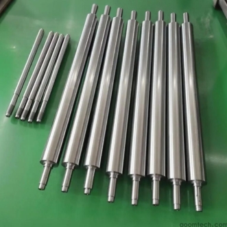
Turning is used for cylindrical semiconductor parts such as shafts, bushings, and precision spacers. These parts require extremely high concentricity and surface finish quality.
During turning, tool selection is critical. Diamond-coated or ultra-fine carbide tools are often used to achieve stable cutting performance. Feed rates must be carefully controlled to avoid surface waviness and dimensional deviation.
Grinding Processes
Grinding is one of the most important finishing processes in semiconductor equipment manufacturing. It is used to achieve ultra-smooth surfaces and extremely tight dimensional tolerances.
Common grinding methods include:
Surface grinding – for flat, highly precise surfaces
Cylindrical grinding – for shafts and round components
The selection of abrasive materials and proper grinding wheel dressing are essential to maintain cutting efficiency and surface quality. Even small wheel wear can lead to dimensional errors.
Tooling Considerations
In semiconductor machining, tooling for semiconductor equipment part CNC plays a vital role in achieving consistent quality. Because many materials are hard, brittle, or chemically sensitive, advanced cutting tools are required.
Recommended tools include:
Diamond-tipped tools for ultra-hard materials
Polycrystalline diamond (PCD) tools for stable long-term cutting
Ultra-fine carbide tools for precision metals
Tool wear monitoring is essential. Even slight wear can cause dimensional drift or surface contamination. Many factories use in-process monitoring systems or scheduled tool replacement to ensure consistent quality.
Post-Machining Processes
After machining, several post-processing steps are often required to achieve final performance requirements.
Chemical etching – used to remove micro-surface defects or adjust surface properties
Stress-relieving heat treatment – reduces internal stress caused by machining
Electro-polishing – improves surface smoothness and removes microscopic burrs
These treatments improve durability, reduce contamination risks, and enhance vacuum compatibility—critical for semiconductor environments.
Quality Control
Quality control in semiconductor machining is extremely strict. Every part must meet precise dimensional and surface standards before it is approved for use.
Advanced inspection tools include:
Coordinate Measuring Machines (CMMs) – for high-precision dimensional measurement
Scanning Electron Microscopes (SEMs) – for surface defect inspection at micro and nano levels
Atomic Force Microscopes (AFMs) – for ultra-fine surface roughness analysis
Statistical Process Control (SPC) is also widely used. It ensures that machining processes remain stable over time and that any variation is detected early before affecting product quality.
Conclusion
The CNC Machining Process for Precision Parts of Semiconductor Equipment requires a combination of advanced technology, strict process control, and deep material knowledge. From material selection to final inspection, every step must be carefully managed to achieve sub-micron accuracy.
By using advanced CAD/CAM systems, ultra-precision machining methods, specialized tooling, and strict quality control, manufacturers can produce reliable semiconductor equipment parts that meet the demands of modern chip production.
As semiconductor technology continues to advance, machining precision will become even more important, pushing CNC manufacturing toward higher levels of accuracy, stability, and cleanliness.
 Process of Custom High-Precisi
 CNC Machining Parameter Settin
 5 Key Tips for CNC Machining o
 Small-batch Precision Parts 5-